Java Boost Schematic Please Review My Homemade Boost Convert
Schematic_5v boost resources Boost keeley java guitar pedal overdrive tagboardeffects layouts fx Mc34063a pinout, example circuits, datasheet, applications,, 40% off
Schematic Boost Converter Sheet 1 20191024172646 | PDF | Computer
Schematic diagram of the boost converter Simulation schematic. (a): conventional bidirectional boost-buck Clean boost schematic
15. schematic diagram of boost converter.
Boost converter circuit diagram pdfBreadboarding a simple mosfet booster Question about boost schematic...Schematic diagram of the boost converter implementation..
Boost voltage inductor constant variable capacitorA simple dc-dc boost converter circuit using 555 timer ic Boost switchSchematic diagram of the boost converter implementation..
Boost schematic model. source: de almeida et al. (2022) [25
Katana keeley boost layout rev tagboardeffects guitar delayKeeley schematic 4: a schematic circuit of a boost converterSchematic circuit of boost converter..
Boost controller adjustable blueCircuit diagram of boost converter from fig. 3, during the switch is The general schematic of a boost circuitGuitar fx layouts: keeley java boost.

Schematic 500k pull
Mosfet audio amplifier circuit diagramBoost converter schematic diagram Lm2577 boost converter circuit step up datasheet pinout, 59% offSchematic boost converter sheet 1 20191024172646.
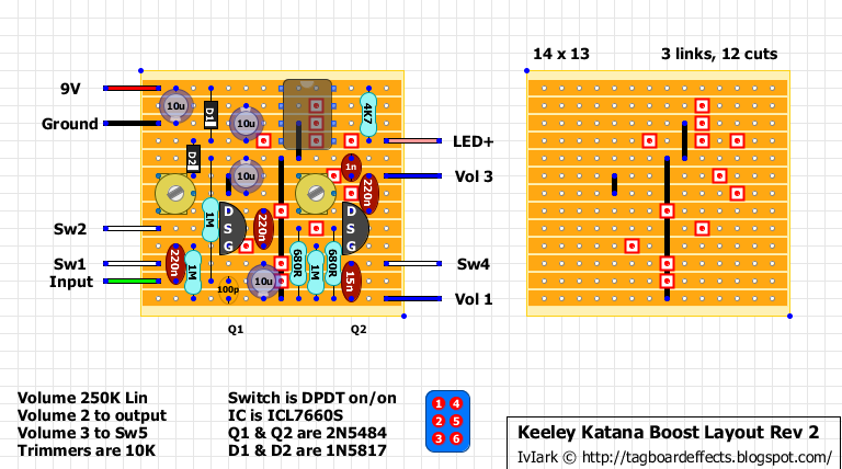
Dc to dc boost converter circuit homemadePlease review my homemade boost converter Guitar fx layouts: keeley katana boost layout rev 2Schema boosteru k el. kytaře (stránka 1).

Boost boost schematic diagram
Keeley katana boost schematicStudy on power electronics, duty cycle of a power electronics system Voltage booster circuit diagramBoost converter schematic diagram.
Circuit diagram of boost converterMosfet booster amz breadboarding barbarach .


Keeley Schematic

Boost Controller Adjustable Blue | SAAS Automotive
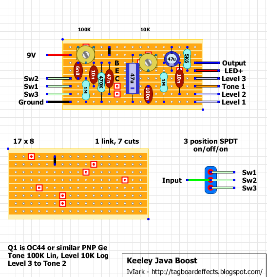
Guitar FX Layouts: Keeley Java Boost

Schematic circuit of Boost Converter. | Download Scientific Diagram

15. Schematic diagram of BOOST converter. | Download Scientific Diagram

Circuit diagram of boost converter From Fig. 3, during the switch is

Boost schematic model. Source: De Almeida et al. (2022) [25

Simulation schematic. (a): Conventional bidirectional boost-buck